Friday, October 31, 2014

6 to 15V DC to DC Converter

A very efficient 6V to 15V DC to DC converter using LM2585 is shown here. LM2585 is a monolithic integrated voltage converter IC that can be used in various applications like flyback converters, boost converters, forward converters, multiple output converters etc. The circuit requires minimum number of external components and the IC can source up to 3A output current.

 
6 to 15V DC to DC Converter Circuit diagram :


dc-to-dc-converter-Circuit
6 to 15V DC to DC Converter Circuit Diagram

Here the IC is wired as a boost converter where resistors R1 and R2 are used to set the output voltage .The junction of R1 and R2 is connected to the feedback pin of IC1. Capacitor C4 is the input filter while capacitor C1 the filter for output. Network comprising of resistor R1 and capacitor C2 is meant for frequency compensation. Inductor L1 stores the energy for acquiring boost conversion.
Notes:    
  • Assemble the circuit on a good quality PCB.
  • LM2585 requires a heatsink.
  • Output voltage is according to the equation Vout =( (R1/R2)+1) x 1.23.
  • Capacitors other than C4 and C1 are ceramic capacitors.
  • Maximum output current LM2585 can source is 3A. 

Source : Circuitstoday

Triac Optimization Circuits


Advanced power control systems make use of electronic plans like Thyristors pro power switching, part control, grinder and so forth. These diplomacy and realize applications participating in inverter design, ability control in lamps, quickness control of motors and so on.

Triacs are the largely general semiconductor procedure used in power control and switching applications. The electronic power control circuits are designed to control the distribution before levels of AC or DC power sources. Such power control circuits can exist used to manually switch power to electrical strategy otherwise to switch power inevitably after parameters such while heat before light intensities try away from fixed level Triac or else Triode intended for alternating current is an electronic device equivalent to two silicon controlled rectifiers together hip inverse like (but with polarity reversed) with their gates connected as one.

Triac
Triac Optimization Circuit | Click image to view larger
This results in a ‘bi-directional electronic switch’, which can conduct current in either direction after triggered. Like SCR, Triac is besides a three terminal device. The MT1 and MT2 (key Terminals 1 and 2) terminals are used to pass current inside either direction while the third terminal G ( gate ) is used to fire trigger pulse to the device.

Triac can live triggered by either a sure before unconstructive voltage functional to its gate electrode. as soon as the voltage on the MT2 terminal is positive with respect to MT2 and a positive voltage is functional to the gate, the ‘missing SCR’ appearing in the triac conducts. If the voltage is reversed and a unconstructive voltage is useful to the gate, the’ authentic SCR’ conducts. tiniest holding current ‘Ih’ have to befall maintained to keep the triac conducting.

AC otherwise DC pulses can trigger Triac and four modes of triggering are probable:
  • Conclusive voltage to MT2 and positive pulse to gate
  • Positive voltage to MT2 and off-putting pulse to gate
  • Negative voltage to MT2 and positive voltage to gate
  • Negative voltage to MT2 and negative voltage to gate

Triacs are borne with a few inherent drawbacks, which wish chew on featuring in their working. conscientious crafty of triac based circuits impart better performance in their working. The central drawbacks of Triacs are Rate effect, RF interference Backlash effect and so forth.

Triac Rate Effect
Involving the MT1 terminal and gate of a triac, an’ home capacitance’ exists. If the MT1 terminal is supplied with a sharply increasing voltage, it causes as much as necessary gate voltage break through to trigger the triac. This condition is referred to equally ‘Rate Effect’, an surplus effect caused generally by the lofty transients during the AC line. Rate effect furthermore occurs as soon as the load is switched on due to high ‘inrush voltage’.

Rate effect is awful particularly in driving inductive heaps such as motor since the load current and voltage are ‘old hat of point’. An R-C Snubber arrangement desire curtail the rate effect and makes the switching clean. The R-C Snubber network is connected connecting the MT2 and MT1 terminals of triac to the same extent exposed happening the assume.

Means of communication Frequency Interference (RFI)
Unwelcome RF generation is an extra chief crisis encountered in triac switching. both stretch the triac is gated on its load, the load current switches sharply from nothing to a from top to bottom price depending on the load resistance and supply voltage. This switching clash (now a hardly any microseconds) generates a pulse of RF1. It is slightest as the triac is triggered close to 00 and 1800 nil crossing points but most in 90 0 wave form. This is as by the side of 00 and 1800 nought crossing points, ‘switch on current’ is lowest possible.

Switch on current is most on 900 producing very high RFI. The strength of RFI is proportional to the chunk of the wire between the load with the triac. The RFI is irritating particularly arrived lamp dimmer circuits and can be situated eliminated using a austere L-C- RFI suppression group.

Backlash Effect
A serious ‘Control Hysteresis’ otherwise ‘Backlash’ develops in triac controlled lamp dimmer circuits, what time the gate current is controlled by a adjustable potentiometer. while the resistance of pot measuring device increases to utmost, the brightness of the lamp reduces to lowest amount. similar to this, the lamp in no way turns on turn over the resistance of the pot measuring device is on sale to a not many ohms, say 50 to 70 ohms. This occurs due to the discharging of capacitor connected to the Diac.

Whilst the triac fires, capacitor discharges by the Diac and generate the ‘backlash effect’. This crisis can be situated clearly rectified by involving a 47 to 100 ohms resistor fashionable cycle with the Diac otherwise count a capacitor (C2) to the gate of the triac. This capacitor (C2) preference stupid down the backlash effect and the packed excursion effect can be located obtained. The connection of capacitor is exposed in map.

20 000 Watt Audio Amplifier Scheme collections

Collection of VersatileAudioAmplifier Number 2

Schema 20kW audio amplifier

Scheme 2000 Watt Audio Amplifier

Scheme 200 Watt Audio Amplifier


Scheme 20 Watt Audio Amplifier

layout PCB


Scheme 2 Watt Audio Amplifier

275W RMS Power Amplifier

275W
The 275W RMS Power Amplifier design includes not simply the final stage of the source (rectifier, filter) and protection aligned with DC voltage output amplifier and spokeswoman links delayed. like already mentioned, the amplifier is designed as a single-module. This instrument so as to on individual universal board rectifier, filter capacitors, protection And beyond doubt amplifier. This transistor provides a thermal criticism and along these lines of a committed quiescent current amplifiers. Privacy speakers are powered immediately from the voltage amplifier. for example pro mechanical design, is probably the a good number complicated now the in one piece amplifier. Cooling is through by the Al blocks with the purpose of are attached to the highest cooling profile. ZH6465 profile is used. The terminal transistors to section is released through Al strips with a thickness of 6 mm in the lateral beams and momentary into the cooler. other pictures.

 275w rms power amplifier
Circuit Diagram 275W RMS Power Amplifier Click image to view High Resolution

Diagram IR Remote Control Circuit using Op amp 741

IR circuit is called Infrared Circuit. Remote controlsare
very much popular now-a-days. It is specially called cordless circuit.
This circuit is very simple and low cost cordless remote control circuit
which is based on
infrared   rays.

Figure 1 shows thetransmitter circuit. The transmitter produces infrared rays and that can be easily transmitted up to 4 meters with a special convex lens and a twin LEDarrangements.
Figure 2 shows thereceiver circuit. Op amp IC1-741 generates high frequency squire wave which provides the gate pulses for SCR1. IC1’s output current flows through  SRC1 and it is conducting current and enables the LED to emits infrared rays. The output frequency of Op amp IC1 depends on the variable resistor VR1, which in turns varies the output radiations of the LED.


When IR rays
fall on the photo-transistor T1 of the receiver, then base of the
photo-transistor’s base produces charge carriers at a rate depending on
the rate of arrival of incident
radiationsat
the pn junction of the transistor. Then the resulting emitter voltage
is amplified by Op amp IC-2 . The amplified signal is rectified by D2.
Finally the amplified signal is to drive the relay.

Parts List:

Thursday, October 30, 2014

AM Receiver Circuit Diagram


This is a compact three transistor, regenerative receiver with fixed feedback. It is similar in principle to the ZN414 radio IC which is now no longer available. The design is simple and sensitivity and selectivity of the receiver are good.

Circuit diagram
Circuit

Notes:
All general purpose transistors should work in this circuit, I used three BC109C transistors in my prototype.The tuned circuit is designed for medium wave. I used a ferrite rod and tuning capacitor from an old radio which tuned from approximately 550 - 1600kHz. Q1 and Q2 form a compund transistor pair featuring high gain and very high input impedance. This is necessary so as not to unduly load the tank circuit.

The 120k resistor provides regenerative feedback,between Q2 output and the tank circuit input and its value affects the overall performance of the whole circuit. Too much feedback and the circuit will become unstable producing a "howling sound". Insufficient feedback and the receiver becomes "deaf". If the circuit oscillates,then R1s value may be decreased; try 68k. If there is a lack of sensitivity, then try increasing R1 to around 150k. R1 could also be replaced by a fixed resisor say 33k and a preset resistor of 100k. This will give adjustment of sensitivity and selectivity of the receiver.

Transistor Q3 has a dual purpose; it performs demodulation of the RF carrier whilst at the same time, amplifying the audio signal. Audio level varies on the strength of the received station but I had typically 10-40 mV. This will directly drive high impedance headphones or can be fed into a suitable amplifier.

Construction:
All connections should be short, a veroboard or tagstrip layout are suitable. The tuning capacitor has fixed and moving plates. The moving plates should be connected to the "cold" end of the tank circuit, this is the base of Q1, and the fixed plates to the "hot end" of the coil, the juction of R1 and C1. If connections on the capacitor are reversed, then moving your hand near the capacitor will cause unwanted stability and oscillation.

Finally here are some voltagee checks from my breadboard prototype.This should help in determining a working circuit:-
All measurements made with a fresh 9volt battery and three BC109C transistors with respect to the battery negative terminal.

Parts
Q1 (b) 1.31V
Q2 (b) 0.71V
Q2 (c) 1.34V
Q3 (b) 0.62V
Q3 (c) 3.87V

CD Rom Drive as Digital Audio CD Player

A CD-ROM drive can be used as a stand-alone unit for playing digital audio CDs without interfacing with a computer. The stereo output of CD player available at the audio jack can be amplified using audio input facility which is normally available on a tape-deck/tape-recorder or a stereo amplifier. Audio socket on front/rear of the CD-ROM drive is capable of driving headphones or speakers of less than 500mW. Proper stereo jacks for interconnection between CD-ROM drive and tape deck are available from computer/tape recorder spares vendors. The principle of operation is illustrated here with the help of block diagram. The 4-pin power supply socket available at the rear of a CD-ROM player is meant for +5V, ground (two middle pins) and +12V inputs. The power supply can be easily derived using a conventional power supply circuit as shown in the figure. If you have an external CD-ROM drive, it can be simply plugged into the mains since it has self-contained power supply circuit inside.

CD-RomWhile there may be minor differences amongst the available CD-ROM drives’ external controls, a typical drive’s controls are shown in the figure here. Please ensure that a proper power supply connector available from computer spare parts vendor is used for connection to CD-ROM drive. To identify +5V and +12V pins on the drive connector, please note that in the computer +12V is routed using a yellow wire and for +5V a red wire is used, while for ground black wires are used with the supply connector. Once the power supply has been connected correctly, you will notice that LED indicator on the drive starts flashing. Now the digital audio CD can be loaded after pushing the eject button. A second push of the same button causes retraction of CD carriage into the drive. One can change the track (song) on the CD using play switch on the CD-ROM drive.

Soft Start For Switching Power Supply

Switching power supply whose output voltage is appreciably lower than its input voltage has an interesting property: the current drawn by it is smaller than its output current. However, the input power (UI) is, of course, greater than the output power. There is another aspect that needs to be watched: when the input voltage at switch-on is too low, the regulator will tend to draw the full current. When the supply cannot cope with this, it fails or the fuse blows. It is, therefore, advisable to disable the regulator at switch-on (via the on/off input). until the relevant capacitor has been charged. When the regulator then starts to draw current, the charging current has already dropped to a level which does not overload the voltage source.

Soft Start For Switching Power Supply  Circuit diagram:


Soft

Soft Start Circuit For Switching Power Supply

The circuit in the diagram provides an output voltage of 5 V and is supplied by a 24 V source. The regulator need not be disabled until the capacitor is fully charged: when the potential across the capacitor has reached a level of half or more of the input voltage, all is well. This is why the zener diode in the diagram is rated at 15 V. Many regulators produced by National Semiconductor have an integral on/off switch, and this is used in the present circuit. The input is intended for TTL signals, and usually consists of a transistor whose base is accessible externally. This means that a higher switching voltage may be applied via a series resistor: the value of this in the present circuit is 22 kΩ. When the voltage across the capacitor reaches a level of about 17 V, transistor T1 comes on, whereupon the regulator is enabled.

Source: National Semiconductors

Automatic light activated switch circuit

The circuit can be used for switching OFF a particular lamp or group of lamps in response to the varying ambient light levels. The unit once built can be used for switching OFF a lamp when dawn breaks and switching it ON when dusk sets in. The power supply is a standard transformer, bridge, capacitor network, which supplies a clean DC to the circuit for executing the proposed actions.

Automatic
Automatic light activated switch circuit schematic

The LDR must be placed outside the box, meaning its sensing surface should be exposed toward the ambient area from where the light level is required to be sensed. The circuit can be used as an automatic street light controller system or a simple light activated switch.

Digital Bike Tachometer Circuit


This digital DIY tachometer for bikes uses two reed switches to get the speed information of the bicycle. The reed switches are installed near the rim of the wheel where permanent magnets pass by. The permanent magnets are attached to the wheelspokes and activate the reed switches everytime they pass by it. The speed is digitally displayed.

Electronic bicycle DIY tachometer circuit diagram
Digital

The tachometer circuit works according to this principle; the pulses created by the reed contacts are counted within a certain time interval. The resulting count is then displayed and represents the speed of the bike. Two 4026 ICs are used to count the pulses, decode the counter and control two 7-segment LED display. RS flip-flops U3 and U4 function as anti-bounce.

The pulses arrive at the counter’s input through gate U7. The measuring period is determined by monostable multivibrator U5/U6 and can be adjusted through potentiometer P1 so that the tacho can be calibrated. The circuit U1/U2 resets the counters.

Since batteries are used to power the circuit, it is not practical to support the continous display of speed information. This circuit is not continously active. The circuit is activated only after a button is pressed. At least three permanent magnets must be installed on the wheel. The circuit can be calibrated with the help of another precalibrated tachometer.

10V Switching Regulator Using LM5007

10V
10V Switching Regulator Using LM5007 Circuit Diagram

The circuit diagram shown here is of a 10V switching regulator based on the LM5007 from National Semiconductors. The LM5007 is an integrated step down switching regulator which has all necessary systems required for making a cost effective and reliable switching regulator circuit. The IC is available in MSOP-8, LLp-8 packages and has a lot of built in features like thermal shut down, under voltage lock out, duty cycle limiting, current limiting etc.

The output voltage of this regulator can be adjusted using the resistor R3 and R4. For the given values of R3 and R4 in the circuit diagram, the output voltage will be 10V. The equation governing the output voltage is Vout = 2.5 x (R3+R4)/R4. Resistor R1 sets the switch on time and C4 is the boost boot strap capacitor. Resistor R2 determines the variation of OFF time and C3 is a decoupling capacitor.

Notes.

* The supply voltage can be anything between 12 to 72V DC.
* Output voltage can be adjusted using R3 and R4.
* C1 and C5 are polyester capacitors.
* C1 and C2 must be rated at least 100V.
* R5 and C5 forms a filter network.
* The output current limit of LM5007 is 700mA.

Wednesday, October 29, 2014

Long range FM transmitter

http://www.electronic-circuits-diagrams.com/radioimages/1.gif

The power output of most of these circuits are very low because no power amplifier stages were incorporated.
The transmitter circuit described here has an extra RF power amplifier stage, after the oscillator stage, to raise the power output to 200-250 milliwatts. With a good matching 50-ohm ground plane antenna or multi-element Yagi antenna, this transmitter can provide reasonably good signal strength up to a distance of about 2 kilometres.
The circuit built around transistor T1 (BF494) is a basic low-power variable-frequency VHF oscillator. A varicap diode circuit is included to change the frequency of the transmitter and to provide frequency modulation by audio signals. The output of the oscillator is about 50 milliwatts. Transistor T2 (2N3866) forms a VHF-class A power amplifier. It boosts the oscillator signals’ power four to five times. Thus, 200-250 milliwatts of power is generated at the collector of transistor T2.
For better results, assemble the circuit on a good-quality glass epoxy board and house the transmitter inside an aluminium case. Shield the oscillator stage using an aluminium sheet.
Coil winding details are given below:
L1 - 4 turns of 20 SWG wire close wound over 8mm diameter plastic former.
L2 - 2 turns of 24 SWG wire near top end of L1.
(Note: No core (i.e. air core) is used for the above coils)
L3 - 7 turns of 24 SWG wire close wound with 4mm diameter air core.
L4 - 7 turns of 24 SWG wire-wound on a ferrite bead (as choke)
Potentiometer VR1 is used to vary the fundamental frequency whereas potentiometer VR2 is used as power control. For hum-free operation, operate the transmitter on a 12V rechargeable battery pack of 10 x 1.2-volt Ni-Cd cells. Transistor T2 must be mounted on a heat sink. Do not switch on the transmitter without a matching antenna. Adjust both trimmers (VC1 and VC2) for maximum transmission power. Adjust potentiometer VR1 to set the fundamental frequency near 100 MHz.
This transmitter should only be used for educational purposes. Regular transmission using such a transmitter without a licence is illegal in India

Extend Timer Range For The 555

Anyone who has designed circuits using the 555 timer chip will, at some time have wished that it could be programmed for longer timing periods. Timing periods greater than a few minutes are difficult to achieve because component leakage currents in large timing capacitors become significant. There is however no reason to opt for a purely digital solution just yet. The circuit shown here uses a 555 timer in the design but nevertheless achieves a timing interval of up to an hour! The trick here is to feed the timing capacitor not with a constant voltage but with a pulsed dc voltage. The pulses are derived from the un smoothed low voltage output of the power supply bridge rectifier.

 Extend Timer Range Circuit 

Extend


The power supply output is not referenced to earth potential and the pulsing full wave rectified signal is fed to the base of T1 via resistor R1. A 100-Hz square wave signal is produced on the collector of T1 as the transistor switches. The positive half of this waveform charges up the timing capacitor C1 via D2 and P1. Diode D2 prevents the charge on C1 from discharging through T1 when the square wave signal goes low. Push-button S1 is used to start the timing period. This method of charging uses relatively low component values for P1 (2.2 MΩ) and C1 (100 to 200 µF) but achieves timing periods of up to an hour which is much longer than a standard 555 circuit configuration.


Circuit Source:  CircuitsProject

Clap Sensitive On Off Relay Diagram Circuit

This circuit was intended to activate a relay by means of a hand clap. Further claps will turn-off the relay. An interesting and unusual feature of this project is the 3V battery operation. The circuits sensitivity was deliberately reduced, in order to avoid unpredictable operation. Therefore, a loud hand clap will be required to allow unfailing on-off switching. Q1 acts as an audio amplifier. IC1 timer, wired as a monostable, provides a clean output signal and a reasonable time delay in order to allow proper switching of the following bistable circuit. A discrete-components circuit formed by Q2, Q3 and related parts was used for this purpose, in order to drive the Relay directly and to allow 3V supply operation.


Circuit Diagram:


Clap Sensitive on-off Relay Circuit Diagram


Parts:

R1 = 12K
R2 = 1M
R3 = 6.8K
R4 = 220K
R5 = 2.2M
R7 = 100K
R8 = 22K
R9 = 6.8K
R10 = 100K
Q1 = BC550C
Q2 = BC328
Q3 = BC328
C1 = 220nF-63V
C2 = 22nF-63V
C3 = 220nF-63V
C4 = 22nF-63V
C5 = 22nF-63V
C6 = 47uF-25V
D1 = 1N4148
D2 = 1N4148
B1 = 3V Battery
IC1 = 7555 CMos IC
RL1 = DIL Reed-Relay SPDT
SW1 = SPST Switch
MIC1 = Electret Mic


Notes:

A small DIL 5V reed-relay was used in spite of the 3V supply. Several devices of this type were tested and it was found that all of them were able to switch-on with a coil voltage value comprised in the 1.9 - 2.1V range. Coil resistance values varied from 140 to 250 Ohm. Stand-by current consumption of the circuit is less than 1mA. When the Relay is energized, current drain rises to about 20mA.

Power Amplifier MOSFET 360 W

I propose here a more powerful version of the 200 Wrms 8 ohms AB class power amplifier project. It shares the same concept that the less poweful model : assembled using common compoments (not very expensive), based on traditional diagrams : a symmetrical differential input stage, a cascode stage driver and a MOSFET output stage. The printed circuit board is very compact , and is composed of two subsets : the command stage and the output stage. All resistors are 1/4 watt 1 % metal film (except if otherwise stated). Constant current sources of +/- 1 mA are formed around T5 and T6. The diodes D1 to D6 allow the use of low noise transistors type BC550C and BC560C, the transistors T7 to T10 form the stage driver. The potentiometer P1 allows the adjustment of the quiescent current to 100 mA per output transistor. The symmetrical power supply is entrusted to a large transformer of 750 VA, 2 * 60 volts + bridge rectifier and 8 reservoir capacitors of 4700 µF, which gives an output voltage of + and - 85 volts per rail. A 1000 VA transformer is necessary for maximal continuous output power at 4 ohms. The output power is 360 Wrms under 8 ohms or 550 Wrms under 4 ohms. Distortion is lower than 0,02 %, damping factor is better than 400, signal-noise ratio is 112 db (balanced A at full power), the input sensitivity is 1,2 volts (360 W under 8 ohms).

Diagram : 

The capacitor C3 is not reproduced on the diagram and on the PCB (it is correct).

Proposal of the command stage PCB : 
 
Transistors T9 and T10 must be assembled on a common heatsink with 5° c/w thermal resistance or on the output stage heatsink.

Proposal of the output stage PCB : 

 The points marked A, B and C have to be connected between the two PCBs. The ground (earth) points of PCBs and loudspeaker ground (earth) must compulsorily be connected in star with the 0 Volts of the PSU. The power transistors must be assembled on a heatsink with a termal resistance less than 0.5 ° C/W. They must also be electrically insulated from the heatsink by using a mica insulator + heat-conducting compound or a silicone insulator.

Bandwidth : 
Bandwidth is limited from 5 Hz to 53 Khz (at - 3 db) by the input module (C1, R1, C2, R2). It can be modified according to the application desired. It is useless to increase the bandwidth to the botton (bass) because little useful signal is present at the bottom of the spectrum. In public address sound systems the bandwidth is often limited between 20 and 35 Hz. The loudspeakers are thus protected against too high extreme-bass signals and some more power is available for the remainder of the spectrum. Michael Eveleigh (UK)
 Source : http://users.swing.be/edwinpaij/ampli_mosfet_360_w.htm

On And Off Button Diagram Circuit

In this simple circuit we give the chip a little more attention than usual. It is astonishing what can be built with a 555. We are always infatuated with simple circuits using this IC, such as the one shown here. The 555 is used here so that a single push-button can operate a relay. If you press the button once, the relay is energized. When you press it again the relay turns off. In addition, it is possible to define the initial state of the relay when the power supply is switched on. The design is, as previously mentioned, very simple. Using R1 and R2, the threshold and trigger inputs are held at half the power supply voltage.

Circuit diagram:
On/Off Button Circuit Diagram

When the voltage at the threshold pin becomes greater that 2/3 of the power supply voltage, the output will go low. The output goes high when the voltage at the trigger input is less than 1/3 of the power supply voltage. Because C2, via R3, will eventually have the same level as the output, the output will toggle whenever the push-button is pressed. If, for example, the output is low, the level of the trigger input will also become low and the output will go high! C1 defines the initial state of the relay when the power is applied. If the free end of C1 is connected to Vcc, then the output is high after power up; the output is low when C1 is connected to ground.
Author: Ger Langezaal - Copyright: Elektor Electronics

Using LV47011P car audio amplifier Diagram Circuit

Using the LV47011P audio power amplifier IC designed for 4-channel BTL power amplifier that developed for car audio system we can implement a very simple car audio amplifier electronic project that can produce an output power between 22 and 50 watts on a 4 ohms load .
This LV47011P car audio amplifier electronic project will provide a maximum 22 watts output power per channel on a 4 ohms load using a 14,4 volts DC power supply at 1% THD .
In same conditions , this car audio amplifier electronic circuit project will provide 29 watts output power at 10% THD .
This IC incorporate various functions (standby switch, muting function, and various protection circuit) necessary for car
audio system and also, it has a self-diagnosis function.
For pop noise prevention, it is recommended to use the muting function at the same time when the amplifier is turned on.
When the amplifier is turn off, turn off the power supply after turning on the muting function .
The muted state is obtained by setting pin 22 to the ground potential, enabling audio muting.
The muting function is turned on by the applied voltage of 1V or less to the resistance of pin 22. And the muting function is turn off when this pin opens.
The circuit is packaged in a Sanyo HZIP 25 package and must be heat sinked , to prevent the damage due to over heating .

Tuesday, October 28, 2014

TDA7383 35W Car Quad Audio Amplifier Circuit

The following a 4 x 35 watts channels/quad audio power amplifier circuit based IC TDA7383. The amplifier circuit is designed specifically suitable for car audio system applications. With a fairly large output power per channel, low distortion and low output noise features. Heatsink should be installed on the power IC to avoid excessive heat. There are very simple and easy to build cos only a few additional components outside the IC power.

Circuit 
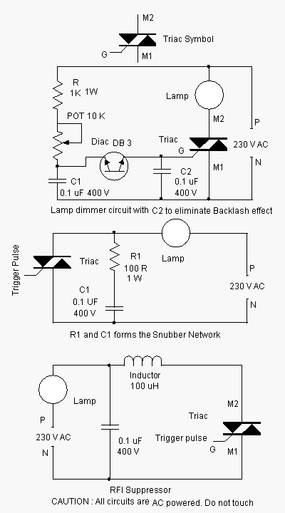
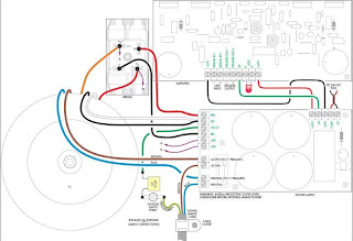
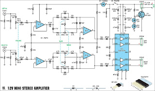
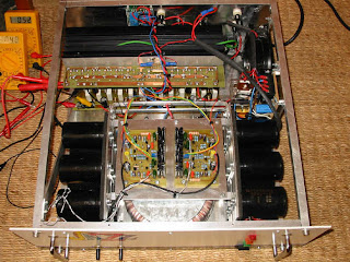
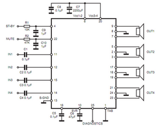
diagram 4 x 35W Car Audio Amplifier TDA7383

IC TDA7383 is a new technology class AB Audio Power Amplifier in Flexiwatt 25 package designed for high end car radio applications. Thanks to the fully complementary PNP/NPN output configuration the TDA7383 allows a rail to rail output voltage swing with no need of bootstrap capacitors. The extremely reduced components count allows very compact sets. The on-board clipping detector simplifies gain compression operations. The fault diagnostics makes it possible to detect mistakes during Car- Radio assembly and wiring in the car.

Absolute Maximum Ratings of IC TDA7383
Operating Supply Voltage : 18 V
DC Supply Voltage : 28 V
Peak Supply Voltage (t = 50ms) : 50 V
Output Peak Current Repetitive (Duty Cycle 10% at f = 10Hz): 4.5 A
Output Peak Current Non Repetitive (t = 100µs) : 5.5 A
Power dissipation, (Tcase = 70°C) : 80 W
Junction Temperature : 150 °C
Storage Temperature : – 55 to 150 °C

Network Voltage Indicator


Using this schematic can be made a network voltage indicator electronic circuit. If the input voltage is present across the network, the optocoupler transistor is open, T1 is blocked and controlled rectifier, Th1, is in a state of conduction. Since both terminals of the piezoelectric buzzer is at the same potential, buzzer is off. If voltage disappears, the transistor T1 enters the conduction and thus makes the terminal of buzzer to be put on the ground (maintains thyristor conduction state).

Network
Circuit Source: DIY Electronics Projects
In this situation, there is a sufficiently large potential difference across the buzzer and D5s to determine that these two elements to indicate AC power loss, both audible and visual. By pressing the reset button current is interrupted by Th1, so thyristor enter in blocking state and the other terminal of the buzzer is connected to ground.

240V to 110V AC Inverter

Using this circuit diagram, can be designed a very simple AC voltage converter, which converts the 240V AC power to a voltage of 110V.

Circuit can be successfully used to power electrical devices that require a supply voltage of 110V. If such a device is a purely resistive load, as electric radiator, letcon the circuit described below will be useful. Basically, this is a regulator that ensures the effective output voltage of 110 V. It can be fixed, of course, at another value for the output voltage, if desired.

The most reliable and accurate method for measuring the load voltage is using a voltmeter with real effective value (which indicates the effective value for voltage harmonic). If the voltage across the load is not correct, we change the value of R2.

240V


Converter can be connected / disconnected from the remote by connecting a switch to 240 volts across REMOTE (jumper will be removed). In this case, command can be done with a voltage of 3-32 V, as shown in diagram. The optocoupler circuit presents the great advantage of isolation of control circuit from the network .

If using a TIC226triac type, the converter can supply currents up to 2 A. If the triac is mounted on a heatsink, the current can reach up to 4 A.

Motorcycle LED Lights Circuit

Motorcycle LED Lights series is so simple that it only uses a few components, but the results are very satisfactory. Power consumption is small enough 6 Volt course is suitable for your motorcycle.

The 555 circuit lower than is a flashing bicycle light powered with four C,D or else AA cells (6 volts). Two sets of 20 LEDs yearn for alternately glimmer by the side of approximately 4.7 cycles for every flash using RC morals publicized (4.7K pro R1, 150K for R2 and a 1uF capacitor). epoch intervals for the two lamps are in this area 107 milliseconds (T1, high LEDs) and 104 milliseconds (T2 junior LEDs). Two transistors are used to provide extra current away from the 200 mA limit of the 555 timer. A single LED is placed in vogue run with the center of the PNP transistor so with the aim of the inferior 20 LEDs ride inedible at what time the 555 output goes superior in the course of the T1 instance interval. The high output level of the 555 timer is 1.7 volts fewer than the supply voltage.

Motorcycle

tallying the LED increases the accelerate voltage mandatory designed for the PNP transistor to a propos 2.7 volts so to the 1.7 volt difference from supply to the output is insufficient to turn on the transistor. both LED is supplied with about 20mA of current for a complete of 220mA. The circuit must labor with bonus LEDs up to about 40 used for both cluster, before 81 total. The circuit resolve too work with fewer LEDs so it possibly will come to pass assembled and tested with righteous 5 LEDs (two groups of two plus solitary) earlier than calculation the others.

NCP2824 bassed Class D amplifier electronic project Diagram Circuit

Using the NCP2824 filterless Class D amplifier can be designed a very simple low power audio amplifier electronic project, capable of delivering up to 2.4 W to a 4 ohms load with a 5 V supply voltage.
With the same battery voltage, it can deliver 1.2 W to an 8 ohms load with less than 1% THD+N. The non−clipping function automatically adjusts the output voltage in order to control the distortion when an excessive input is applied to the amplifier.

This adjustment is done thanks to an Automatic Gain Control circuitry (AGC) built into the chip. A simple single wire interface allows to the non Clipping function to be enabled and disabled.
A programmable power limit function is also embedded in order to protect speakers from damage caused by an excessive sound level.
2.4

Mosfet Power Amplifier 100 Watt

At this time a unsophisticated MOSFET amplifier or else power Amp which Output power is plus/minus 100 Watt/RMS with 8 Ohms otherwise ohter plus/minus 160 Watts /RMS with 4 ohms.

Mosfet
Mosfet Amplifier 100 Watt RMS
Regarding this circuit simplicity, The distortion is plus/minus 0.1 %. In support of mob-width -3 db(decibel) is increase for 4 Hz to 96 Khz, it is narrow by C1, R1, C2 and R2. Taking part in the two transistors are T1 and T2 makes a initial differential stage part, So,current source(I) of +/- solitary mA is put with resistor R3. In favor of the upgraded project, The current source(I) is new efficient in stability. Coil P1 allows a fine tuning of dictate current voltage on amplifier’s output. Place the Coil P1 with it’s partially usefulness in favor of first power up, so therefore break it unhurriedly for a lowest DC output voltage. custom a essential quality compoment.

Electronic Part
C1 = 2,2 µF MKP, MKT 100 in opposition to
C2 = 330 pF céramique 50 V
C3 = 100 nF MKP, MKT 100 in opposition to
C4 = 100 µF 40 V électro-chimique
C5, C6 = 18 pF céramique 50 vs.
C7 = 100 nF MKP, MKT 250 V  (C8 = 47 µF 100 V)
R1, R3 = 47 K   (R3 = 330 -> 470 Ohms)
R2 = 2K2
R4, R5 = 3K9
R6 = 1 K
R7 = 27 K
R8, R9, R11 = 100 ohms
R10 = 10 K
R12, R13 = 470 ohms
R14, R15 = 0.33 ohms 5 watts
R16 = 10 ohms 3 watts      (R17 = 1 K    R18, R19 = 10K)
T1, T2, T9,T10 = 2SD756A,2SD716A, BC556B (attention au brochage différent - take be concerned representing pin arrange)
T7 = IRFP240, 2SK1530, 2SJ162, BUZ900DP, BUZ901DP (attention au brochage dissimilar - take care for pin layout : GDS GSD)P1 = 100 ohms  (25 turns - 25 turns)


Monday, October 27, 2014

Troubleshooting STR IC Regulator Power Supply

A. Unable to start.
Can be caused by:
  • No start-up voltage supply Vcc or a voltage less than 16V
  • Electrolityc Capacitors supply voltage Vcc filter dry.

  
2. Led indicator blinking
If the supply voltage Vcc examined rocking. This is because the regulator of life and death because OVLO work., Die-protectionist regulators and auto start life over and over. If it is turned off  Electrolityc Capacitors  usually still keep the rest of the cargo.
Can be caused by:

  • Electrolityc Capacitors supply voltage Vcc filter on a pin-4 dry. Replace with a value equal to or slightly larger. - triger UVLO
  • input filter capacitor on pin-1 feed dry behind the declining value - triger OLP
  • Rectifier diode of the switching transformer is damaged (sometimes when examined with avo-meter looks like a still good)
  • cause the supply voltage Vcc drops of the switching transformer (UVLO)
  • Part damage or broken lines on the feedback circuit of the voltage regulator through B to photocoupler - triger OVP
  • Electrolityc Capacitors dry filter voltage B - triger OVP
  • One of the output voltage of the switching transformer secondaries there is a short (over load) - triger OLP
  • Soft start capacitor value decreases - triger OLP

3. Noise arising (noise)
Can be caused by:

  • Transformer windings slack.
  • If there are ceramic capacitors - can sometimes cause interference noise due to its characteristic piezoelectrik like crystal resonator. Replace with film capacitors.

4. When the st-by normal stress. But when the power is on the regulator directly off protectionism no voltage on the secondary this part.  Electrolityc Capacitors  are still storing charge.
Can be caused by:

  • Sensor OVP small value resistor on pin-2 to the ground so that the value of delayed triger to OLP or OCP.
  • Regulator IC is damaged

TA8256BH bassed 6 watts 3 channel audio amplifier Diagram Circuit


Using the TA8256BH audio amplifier IC can be designed a very simple 3 channel audio power amplifier for audio applications that require a small power .
This IC provides an output power of 6 watts per channel (at VCC = 20 V, f = 1 kHz, THD = 10%, RL = 8 Ω).

TA8256BH audio amplifier project is suitable for power amplifier of TV and home Stereo.
Some important build in functions of these audio circuit project , based on the TA8256BH are : audio muting circuit , thermal shut down protection circuit, over voltage protection circuit .
TA8256BH power amplifier can operate over a wide range input voltage from 10 to 30 volts .

BC550 High Temperature ALARM

The circuit is small regulatorof temperature, us warns for the increase of temperature. The control of temperature becomes from the thermistor TH1, that is negative factor. His resistance is altered between in the 10K in temperature 25° C and roughly in the 1K in their 94° C. The trimmer TR1 regulates the precise temperature in which the Q1-2, connected as darlington, conduct, making him relay K1 close also the buzzer BZ, sound. The alarm is activated when the temperature becomes bigger than predetermining. The thermistor it should he is placed far from the remainder circuit, in order that this is not in danger from the temperature.

The supply of circuit becomes from battery 9V, but if he is placed in constant place, then we can him supply with one power supply . In the contacts of relay we can connect what load we want, as a lamb, other circuit k.a. Also can is added a LED, if we want to have also optical clue of excitation. The regulation becomes sinking him thermistor TH1, in water which we know the temperature of (the contacts should are well insulate so that do not have short-circuit) and regulating him trimmer, until excited the circuit. The cable that we connect the circuit with the TH1, should be plate.

1W BTL Audio Amplifier Diagram Circuit

The TDA8581(T) from Philips Semiconductors is a 1-watt Bridge Tied Load (BTL) audio power amplifier capable of delivering 1 watt output power into an 8-Wload at THD (total harmonic distortion) of 10% and using a 5V power supply. The schematic shown here combines the functional diagram of the TDA8551 with its typical application circuit. The gain of the amplifier can be set by the digital volume control input. At the highest volume setting, the gain is 20 dB. Using the MODE pin the device can be switched to one of three modes: standby (MODE level between Vp and Vp–0.5 V), muted (MODE level between 1 V and Vp–1.4 V) or normal (MODE level less than 0.5 V). The TDA8551 is protected by an internal thermal shutdown protection mechanism. The total voltage loss for both MOS transistors in the complementary output stage is less than 1 V.

Circuit diagram:1-Watt
1 Watt BTL Audio Amplifier Circuit Diagram

Using a 5-V supply and an 8-W loudspeaker, an output power of 1 watt can be delivered. The volume control has an attenuation range of between 0 dB and 80 dB in 64 steps set by the 3-state level at the UP/DOWN pin: floating: volume remains unchanged; negative pulses: decrease volume; positive pulses: increase volume Each pulse at he Up/DOWN pin causes a change in gain of 80/64 = 1.25 dB (typical value). When the supply voltage is first connected, the attenuator is set to 40 dB (low volume), so the gain of the total amplifier is then –20 dB. Some positive pulses have to be applied to the UP/DOWN pin to achieve listening volume. The graph shows the THD as a function of output power. The maximum quiescent current consumption of the amplifier is specified at 10 mA, to which should be added the current resulting from the output offset voltage divided by the load impedance.

DC Voltage Doubler

The The Circuit of DC Voltage Doubler was designed on arrived type Power Supply. Please study carefully and comprehend by the side of schematic design photos of The Circuit of DC Voltage Doubler to pick up factor in sequence.

DC Voltage Doubler Schematic

This is a economical DC Voltage Doubler Circuit diagram, which requires a hardly any components and strength of character surrender 10V from a 5V power supply. If the oscillator essential be present built from a non-functional gate next is essential 2 supplementary components: R1 and C3. The a large amount principal parameters of this voltage doubler circuit are set arrived the submit less than. memorandum with the aim of as of the IC tolerances these data may possibly contain approximately differences.

Sunday, October 26, 2014

Hi Fi Audio Amplifier Circuit LM1875

This circuit is the audio amplifier circuit has a very common single.This is a austere circuit. insignificant pieces of equipment. And Watt are climax.The circuit uses IC integer LM1875, which is under the protection circuit IC output or else Too condensed circuit. And a sizeable distortion in the same way as low as 0.015% on a frequency of 1kHz.
Hi-Fi Audio Amplifier Circuit LM1875

This circuit uses optimistic, downbeat ground power supply to get a hold the audio hint with both halves of the signal swing, positive and negative halves,The sound with the aim of came unconscious gemstone bright.production is. while paying into the audio input. Audio is through R1, R2, C1 and R3 to limit the audio hint appropriately.And limit the din to the input signal assorted down to the ground.next sends a signal to racket to the input pin of IC 1.A noninterting pin, amplifier non-return point.Out of the 4 output pins to access the speakers.The R6 and C4 eliminate blast assorted with the output down to the ground.And a new part of the audio output pin 4 of integrated circuit want come to pass fed back into place through R5 to pin 2, which R4 and R5 determines the rate of boost up, can be calculated from R5/R4,will secure equal to 15 epoch, With a C2 to touch climax frequencies better.

Car Parking Sensor circuit Using Infra Red LED

This circuit can be used for an assist in parking the car near the garage wall backing up Pls. LED D7 illuminates Pls bumper-wall distance is about 20 cm., D7 + D6 illuminate at about 10 cm. and D7 + D6 + D5 at about 6 cm. In this manner you are alerted Pls approaching too close to the wall.

Car Parking Sensor circuit

All distances mentioned before can vary, depending on infra-red transmitting and receiving LEDs used and are mostly affected by the color of the reflecting surface. Black surfaces lower greatly the device sensitivity. Obviously, you can use this circuit in other applications like liquids level detection, proximity devices etc.

Note:
  • The infra-red Photo Diode D2, should be of the type incorporating an optical sunlight filter: these components appear in black plastic cases. Some of them resemble TO92 transistors: in this case, please note that the sensitive surface is the curved, not the flat one.
  • Avoid sun or artificial light hitting directly D1 & D2.
  • If your car has black bumpers, you can line-up the infra-red diodes with the (mostly white) license or number plate.
  • It is wiser to place all the circuitry near the infra-red LEDs in a small box. The 3 signaling LEDs can be placed far from the main box at an height making them well visible by the car driver.
  • The best setup is obtained bringing D2 nearer to D1 (without a reflecting object) until D5 illuminates; then moving it a bit until D5 is clearly off. Usually D1-D2 optimum distance lies in the range 1.5-3 cm.
List Component of Car Parking Sensor circuit:
R1 : 10K
R2,R5,R6,R9 : 1K
R3 : 33R
R4,R11 : 1M
R7 : 4K7
R8 : 1K5
R10,R12-R14 : 1K
C1,C4 : 1µF/63V
C2 : 47pF
C3,C5 : 100µF
D1 : Infra-red LED
D2 : Infra-red Photo Diode (see Notes)
D3,D4 : 1N4148
D5-7 : LEDs (Any color and size)
IC1 : NE555
IC2 : LM324
IC3 : LM7812

circuit for Digital Stop Watch

Make a Digital Stop Watch

Description

A digital stop watch built around timer IC LM555 and 4-digit counter IC MM74C926 with multiplexed 7-segment LED display.MM74C926 consists of a 4-digit counter, an internal output latch, npn output sourcing drivers for common cathode,7-segment display and an internal multiplexing circuitry with four multiplexing outputs.The counter advances on negative edge of the clock. The clock is generated by timer IC LM555.The circuit works off a 5V power supply. It can be easily assembled on a general-purpose PCB. Enclose the circuit in a metal boxvwith provisions for four 7-segment displays, rotary switch S1, start/stop switch S2 and reset switch S3

Testing

First, reset the circuit by pressing S3 so that the display shows ‘0000.’ Now open switch S2 for the stop watch to start counting the time. If you want to stop the clock, close S2. Rotary switch S1 is used to select the different time periods at the output of the astable multivibrator (IC1).

Digital Timer Circuit Diagram .

Click to View in full size.

stopwatch-1.JPG

You may also be interested in other Timer circuits we have in our website:

1. Long Duration Timer Circuit

For more circuits, please check our category on Clocking and Timer Circuits

74LS192 Computer controller 4 DC motors


This circuit has proven useful when interfacing my computer to home made robotics. It is easy to build and use and it can control two DC motors of any current or voltage rating, depending on the rating of the relays. The circuit also provides two shaft encoders for positional feedback to the computer.

Saturday, October 25, 2014

Speaker to microphone converter Diagram Circuit

Description.
This circuit is a simple approach for converting a loud speaker into a microphone. When the sound waves fall on the diaphragm of a speaker, there will be fluctuations in the coil and there will be a small proportional induced voltage. Usually this induced voltage is very low in magnitude and useless. Here in the circuit the low voltage is amplified using transistors to produce a reasonable output. The transistor Q1 is wired in common base mode and produces the required voltage gain. The transistor Q2 is wired as an emitter follower to produce enough current gain. The voice quality of this circuit will not be as much as a conventional microphone but quite reasonable quality can be obtained. To set up the circuit, keep the preset R2 at around 10 Ohms and connect the battery. Now adjust R2 to obtain the optimum sound quality.
Circuit diagram with Parts list.


Notes.
  • Assemble the circuit on a general purpose PCB.
  • Power the circuit from a 9 V PP3 battery.
  • A 3 inch speaker can be used as K1.
  • All capacitors must be rated at least 15V.
  • An 8 Ohm speaker or head phone can be connected at the output to hear the picked sound.